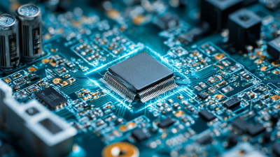
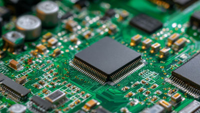
How to Effectively Design PCB Circuit Boards for Optimal Performance
The design of PCB circuit boards has evolved significantly over the past few years, driven by advancements in technology and the increasing demand for high-performance electronics. The global printed circuit board market is projected to reach $82.5 billion by 2026, according to a report by Mordor Intelligence, highlighting the essential role that effective PCB design plays in the performance and reliability of electronic devices. As industries incorporate more sophisticated features into their products, the importance of optimizing PCB circuit board design cannot be overstated.
In this competitive landscape, designers face numerous challenges, including miniaturization, signal integrity, and thermal management. A comprehensive understanding of the latest design methodologies and technologies is crucial for engineers to create PCBs that not only meet current performance standards but also anticipate future demands. For instance, a survey conducted by IPC indicates that nearly 70% of manufacturers prioritize efficiency in PCB design to enhance product lifecycle and minimize production costs. This underscores the necessity for engineers to adopt best practices in PCB circuit board design to ensure optimal performance and maintain market competitiveness.
By focusing on key design principles and leveraging emerging technologies, such as advanced simulation tools and automation, designers can produce high-quality PCB circuit boards that deliver superior performance. This article aims to provide insights into the top strategies and techniques that will help professionals design effective PCBs and ultimately achieve optimal performance in their applications.
Understanding the Basics of PCB Design Principles for High Performance
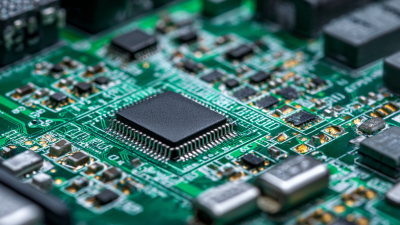
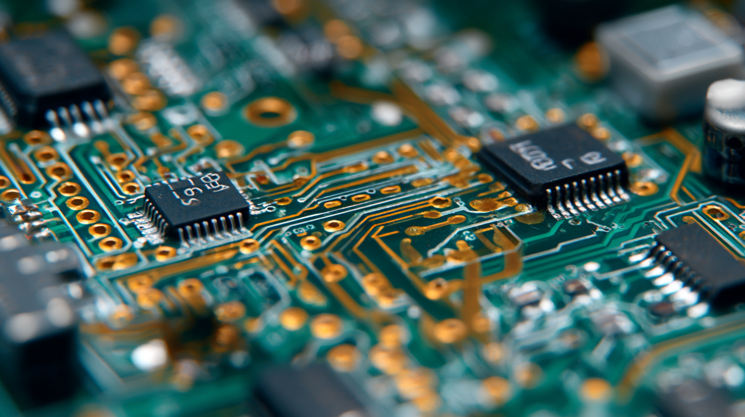
 Understanding the basics of PCB design principles is crucial for achieving high performance in electronic devices. One of the foundational aspects is to maintain a clear and organized layout, which helps to minimize electromagnetic interference and signal degradation. Designers should ensure that traces are appropriately sized and spaced to handle the intended current without excessive voltage drops. Additionally, using a ground plane can greatly enhance the performance by providing a low-resistance path for return currents and reducing noise.
Another important principle is proper component placement. Strategically placing components close to their function can reduce the length of the traces, which is critical for high-speed applications. It's also vital to consider thermal management during the design process; components that generate significant heat should be placed in areas with adequate ventilation and away from heat-sensitive parts. By adhering to these principles, PCB designers can create effective circuit boards that not only perform well but also enhance the overall reliability and longevity of the electronic devices.
Selecting the Appropriate Materials for Enhanced Electrical Characteristics
Selecting the right materials for PCB circuit boards is crucial for achieving enhanced electrical characteristics and optimal performance. The choice of substrate materials, such as FR-4, polyimide, or ceramic, can significantly influence thermal management, dielectric properties, and overall lifespan of the circuit board. Each material comes with its unique set of advantages that can better suit specific applications, such as high-frequency communication or demanding industrial environments.
Tips: When choosing materials, consider the frequency and power requirements of your application. Higher frequencies may necessitate materials with lower dielectric loss, while environments requiring high thermal conductivity should look towards specialized substrates. Additionally, consider the environment in which the PCB will operate; materials resistant to moisture, chemicals, and temperature fluctuations are essential for durability.
Another critical aspect is the selection of conductive materials. Copper is the standard, but for high-performance applications, alternatives like gold or silver may be warranted. The thickness of the copper layer affects both the current-carrying capacity and the heat dissipating ability of the PCB.
Tips: Evaluate the trade-offs between cost and performance when selecting conductive materials. More expensive options may yield better performance but weigh the long-term benefits against the initial expenditure. Proper adherence to these material selection guidelines will ensure not only an efficient and functional PCB design but also reliability in its intended application.
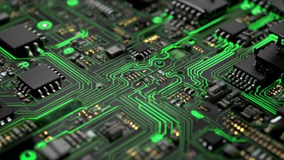
Optimizing Layout and Component Placement for Signal Integrity
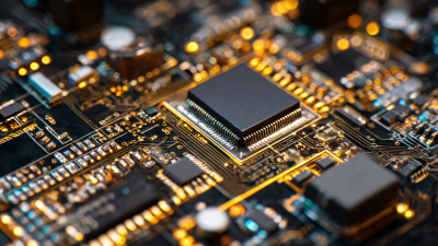
When designing PCB circuit boards, the layout and component placement are critical factors that directly influence signal integrity. A well-thought-out arrangement minimizes parasitic capacitance and inductance, which can distort signal waveforms and reduce performance. Placing high-speed signals close together and routing them on the same layer helps to maintain a consistent return path, thereby enhancing signal clarity. Additionally, using controlled impedance traces ensures that signals are transmitted without excessive reflection, preserving the integrity of the data being communicated.
Furthermore, careful consideration of power distribution and ground planes is essential in optimizing PCB design. A solid ground plane can act as a shield, reducing electromagnetic interference while providing a low-resistance path for return currents. It's also vital to decouple capacitors strategically and to position them near power pins of components to isolate noise and stabilize voltage levels. By harmonizing the layout with these principles, designers can achieve optimal performance and reliability in their PCB designs, ultimately leading to more robust electronic products.
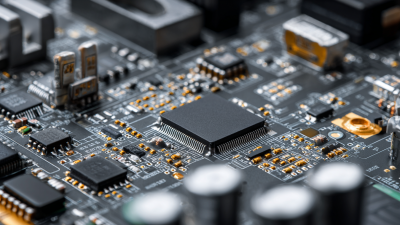
Implementing Effective Thermal Management Techniques in PCB Design
Effective thermal management is crucial in PCB design to ensure optimal performance and longevity of electronic devices. According to a report by the IPC (Association Connecting Electronics Industries), improper thermal management can lead to a significant decrease in component reliability, with studies showing that for every 10°C increase in operating temperature, the failure rate of electronic components can double. Thus, implementing effective thermal management techniques is fundamental for preventing overheating and maintaining efficiency.
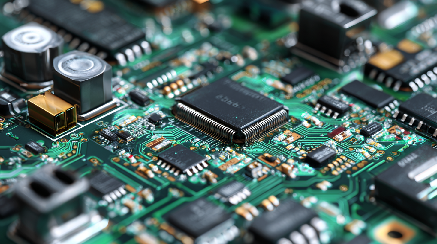
One essential technique is to utilize thermal vias, which can help dissipate heat away from high-temperature areas, promoting better thermal conductivity. Another approach is to strategically place components, ensuring that heat-sensitive parts are distanced from heat-generating elements, such as voltage regulators or power transistors.
**Tips:** Consider using copper pour areas to enhance heat spreading across the PCB. It's also beneficial to select materials with a higher thermal conductivity, such as aluminum or ceramic substrates, especially for high-power applications. Regular thermal analysis during the design phase can prevent long-term performance issues and enhance reliability.
How to Effectively Design PCB Circuit Boards for Optimal Performance - Implementing Effective Thermal Management Techniques in PCB Design
| Design Aspect |
Technique |
Impact on Performance |
Recommended Practices |
| Thermal Dissipation |
Heat Sinks |
Improves heat dissipation, reduces overheating |
Use larger heat sinks; ensure good thermal contact |
| Circuit Layout |
Component Spacing |
Prevents localized heating |
Maintain adequate spacing between components |
| Power Management |
Power Planes |
Distributes power evenly, reduces current density |
Use sufficient ground and power planes |
| Material Selection |
Thermal Conductive Materials |
Enhances heat transfer |
Choose materials with high thermal conductivity |
| Simulation Tools |
Thermal Analysis Software |
Predicts thermal behavior under different operating conditions |
Utilize simulation tools during design stages |
Testing and Iterating Designs for Continuous Improvement and Reliability
In the realm of printed circuit board (PCB) design, testing and iterating designs are crucial for enhancing performance and ensuring reliability. According to a report by IPC, rigorous testing can reduce the likelihood of early failures by up to 50%. By employing methods such as Design for Testability (DFT) and validating designs through simulation tools, engineers can identify potential issues early in the development process. This proactive approach allows for modifications based on real-world scenarios, ultimately leading to more robust products.
Furthermore, continuous improvement is facilitated through iterative design cycles. A study published in the Journal of Electronic Packaging indicates that companies adopting Agile methodologies in their PCB design process experience 30% faster time-to-market while maintaining higher quality standards. By incorporating feedback from testing phases into subsequent iterations, designers can refine their boards to meet evolving performance specifications and adapt to new technologies. Implementing continuous testing, such as Automated Optical Inspection (AOI), ensures defects are caught early, minimizing costly changes late in the production life cycle.