How to Print PCB Board at Home for Your Electronics Projects?
In the realm of electronics, the ability to print PCB boards at home empowers creators and innovators alike. Renowned expert Dr. Alice Wang, a leading figure in PCB technology, once stated, "The journey of creating custom circuits begins with understanding the printing process." This illustrates the significance of mastering PCB printing for DIY electronics projects.
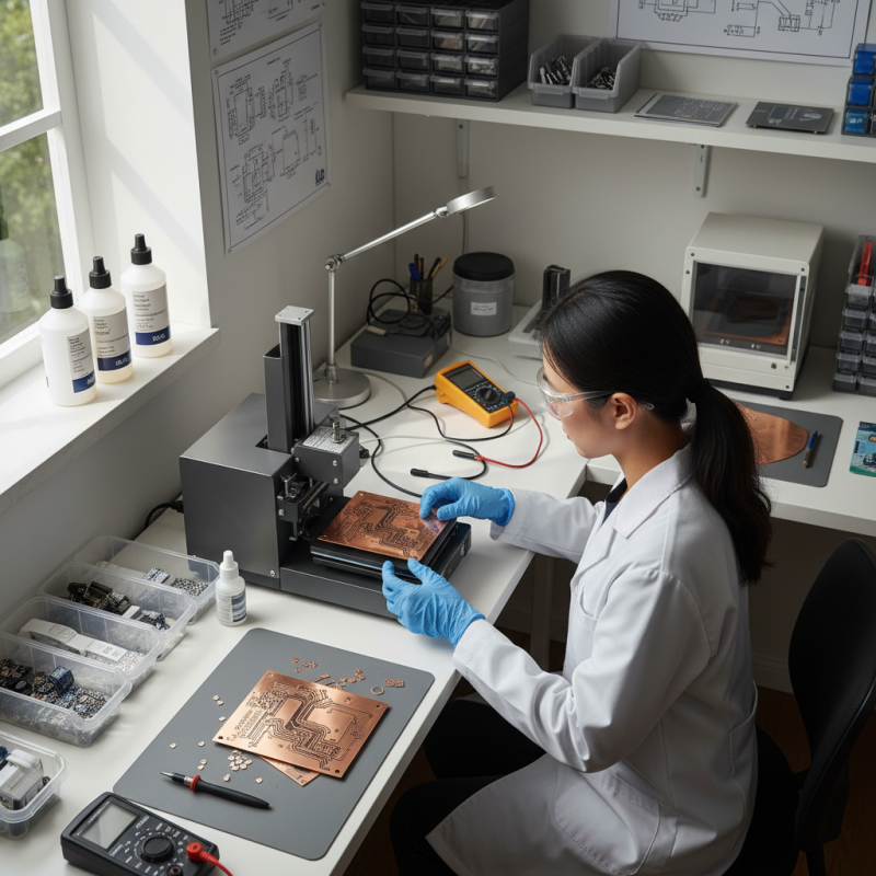
Printing PCB boards involves precision and attention to detail. It’s crucial to select the right materials and tools. Mistakes can lead to faulty boards and wasted time. Preparing a clean workspace is essential. Without proper arrangement, the process can become chaotic and frustrating.
Although the process can seem straightforward, challenges persist. Test prints may reveal flaws that require reflection and adjustment. Each printed board is an opportunity to learn. As you strive to perfect your technique, remember: persistence is vital. Embrace the learning curve inherent in this craft, and you will become adept at printing PCB boards.
Choosing the Right Materials and Tools for PCB Printing at Home
When considering PCB printing at home, choosing the right materials and tools is crucial. A high-quality printer can significantly impact your results. Industry reports suggest that laser printers are often recommended. They provide better resolution compared to inkjet printers. A laser printer can create finer traces, which improves circuit reliability.
Moreover, using specialized PCB paper enhances the transfer of your design to the copper board.
Another essential element is the etching solution. Ferric chloride is commonly used for etching PCBs. It efficiently removes unwanted copper and produces cleaner results. However, working with chemicals carries risks. Proper ventilation and protective gear are necessary. Homemade solutions can also be less effective.
A balance of cost and quality is vital when sourcing materials. Additionally, consider the copper-clad board type. FR-4 is popular due to its thermal and electrical properties. Yet, it can be challenging for beginners. A beginner might opt for a pre-sensitized board to simplify the process.
Be ready for some trial and error. Not every attempt will yield perfect results. Reflect on the failures, as they often lead to better techniques and improved outcomes. The learning curve is steep, but perseverance pays off.
Preparing Your PCB Design Using Software for Home Printing
Creating a printed circuit board (PCB) at home can be a rewarding task. The first step is designing your PCB layout. Software like KiCAD or Eagle can assist in this process, allowing you to visualize your circuit. According to a 2020 industry report, over 50% of hobbyists use software tools for PCB design, emphasizing their importance in DIY electronics.
When using PCB design software, pay attention to the software's design rules and capabilities. For instance, making sure your traces meet the minimum width is crucial. An article from PCB Design Magazine highlighted that 60% of failed home PCBs stem from poor trace design. Ensure your components are properly placed, minimizing overlap and maximizing space.
Once your design is ready, exporting it as a Gerber file is key. This file format is a standard in PCB manufacturing. However, many users overlook this step, leading to unexpected issues. Testing the design before printing is essential. A practice that many learn through experience is that not every detail translates well during the printing process. Minor adjustments can lead to significant improvements in the final product.
The Step-by-Step Process of Printing PCBs at Home
Printing PCBs at home can be a rewarding yet challenging experience. It begins with designing your circuit board. Use simple software to create a layout. Ensure the design is clear and easy to follow. Mistakes in the layout can lead to circuit failures, so double-check every connection.
Next, prepare your materials. You’ll need copper-clad boards, a printer, and a transfer method. Laser printers work well for this task. The transfer process can be tricky. Getting the right heat and pressure can be hit or miss. Sometimes the copper doesn’t transfer fully, and you might end up with incomplete traces. If this happens, don’t get discouraged. It’s a normal part of the learning curve.
Once the transfer is complete, etch your board using a suitable solution. Follow safety precautions during this step. You might notice uneven etching or stray copper bits left behind. Addressing these imperfections will require careful work with a fine tool. These small details can make or break your project. Patience is crucial.
How to Print PCB Board at Home for Your Electronics Projects? - The Step-by-Step Process of Printing PCBs at Home
| Step |
Description |
Materials Needed |
Estimated Time |
| 1 |
Design your PCB layout using software. |
PCB design software (e.g., KiCAD, Eagle) |
1-2 hours |
| 2 |
Print the PCB design onto a transfer paper. |
Laser printer, transfer paper |
30 minutes |
| 3 |
Prepare the copper board by cleaning it. |
Copper board, cleaning solution |
15 minutes |
| 4 |
Transfer the design onto the copper board. |
Iron, transfer paper |
10 minutes |
| 5 |
Etch the copper board to create the circuit paths. |
Etching solution, gloves |
30 minutes |
| 6 |
Clean and drill holes for components. |
Drill, cleaning solution |
20 minutes |
| 7 |
Solder the electronic components onto the PCB. |
Soldering iron, solder, components |
1 hour |
| 8 |
Test the finished PCB to ensure functionality. |
Multimeter, testing tools |
30 minutes |
Etching and Finalizing Your Printed Circuit Board
Etching your printed circuit board (PCB) is a crucial step in the home production process. After designing your PCB, the next phase involves transferring the design onto a copper-clad board. You can achieve this through various methods, such as using a UV light box or even the toner transfer method. Each technique has its pros and cons. The quality of your etching can significantly impact the board’s performance, so be mindful of details.
Once the design is transferred, it’s time to etch the board. This involves submerging the board in an etching solution, often ferric chloride. It’s important to monitor the process closely. Over-etching can ruin your design. Under-etching may leave copper traces, which can lead to short circuits. After etching, rinse the board to remove the solution. Take a moment to inspect your work. You might find some imperfections that need adjustments.
The last step is finalizing your PCB. This includes drilling holes for components and cleaning the board. A clean board is essential for proper soldering. You might face challenges, like uneven etching or misaligned holes. Don’t rush this process; take time to reflect on what works and what doesn’t. Each mistake is a learning opportunity. Ultimately, creating PCBs at home requires patience and practice.
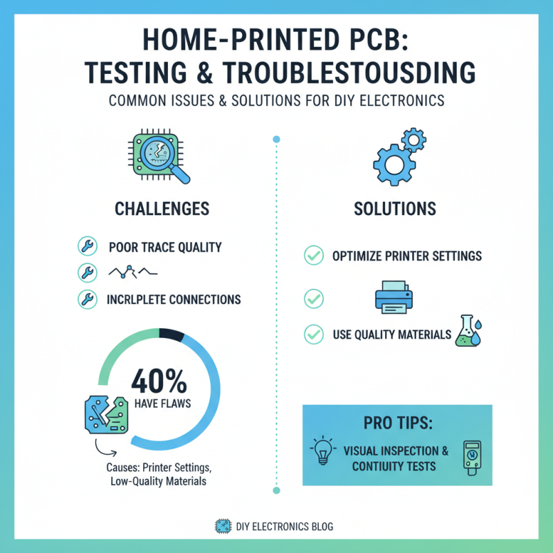
Testing and Troubleshooting Your Home-Printed PCB
When printing a PCB at home, testing and troubleshooting are crucial. Many DIY enthusiasts face common issues like poor trace quality or incomplete connections. Statistics show that nearly 40% of home-printed PCBs have some kind of flaw. These issues can stem from various factors, such as incorrect settings on the printer or using low-quality materials.
To troubleshoot effectively, first check your printer's calibration. This step can significantly impact the print quality. Use a micrometer to measure the width of traces. Ideally, traces should be around 0.25 mm. If they are too thin or uneven, you may need to adjust your design software settings or switch to a better printing paper. It’s vital to perform tests on several prototypes before finalizing a design.
Another common issue is soldering problems. Poor solder connections can lead to circuit failures. Utilize a multimeter to test for continuity across your components. Some reports indicate that over 30% of solder-related failures occur due to inadequate heating. Slow and steady soldering practices can improve your results. Troubleshooting takes time, and it’s essential to reflect on your processes to improve future projects.