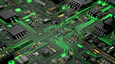
2026 How to Understand PCB Fabrication and Assembly Process?
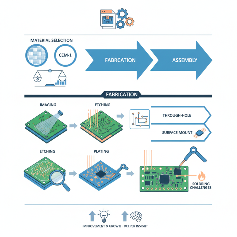
Understanding the PCB fabrication and assembly process is crucial for anyone in electronics. It involves transforming design files into functional printed circuit boards. This complex journey begins with material selection, where choices like FR-4 and CEM-1 are considered. Each material affects performance and cost.
The fabrication stage encompasses imaging, etching, and plating. It's a delicate dance of precision and accuracy. Mistakes in this phase can lead to costly reworks. For example, misalignment during etching can create faulty circuits. Attention to detail is vital.
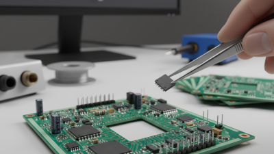
After fabrication, assembly takes place. Here, components are placed on the boards. Techniques include through-hole and surface mount assembly. Each method has its pros and cons. Challenges arise in soldering, especially in high-density designs. Understanding these processes deepens insight into PCB production, revealing areas for improvement and growth.
Overview of PCB Fabrication and Assembly Processes
The PCB fabrication and assembly processes are critical in electronics. These processes transform design into a functional printed circuit board. Understanding these stages is essential for engineers and hobbyists alike.
PCB fabrication begins with the creation of a substrate. Copper is layered onto the substrate and etched to form the circuit pathways. This process involves multiple steps, such as drilling, coating, and plating. Each step has its challenges. For example, ensuring precise drilling can be tricky. Over-drilling can lead to circuit failures or faults.
Once fabrication is complete, assembly comes next. Components are placed onto the PCB, often using automated machines. Soldering then secures these components. However, inaccuracies during placement can result in defects. Manual inspection may be needed, but it can be time-consuming and prone to human error. Balancing automation with quality checks remains a challenge for many manufacturers.
Key Steps in the PCB Fabrication Process
The PCB fabrication process is intricate and requires precision. The essential steps begin with designing the layout. Engineers use software to create a detailed design that dictates the circuitry. It includes components, connections, and layers. Each detail matters in the outcome.
Next, the fabrication begins. The design is transferred to a substrate, often made of fiberglass. Layers of copper are added through processes like etching. This is where mistakes may happen. If the design isn’t accurately transferred, it leads to defects. Quality control is crucial at this stage.
After fabrication, assembly follows. Components are placed on the board. Soldering techniques are applied to create strong connections. Each step can introduce errors. Sometimes, components may be misplaced or improperly soldered. Ensuring high quality requires constant monitoring and adjustments. Innovations in methods help improve these processes. Yet, there’s always room for reflection on efficiency and accuracy.
PCB Fabrication Process: Key Steps Overview
This chart illustrates the key steps involved in the PCB fabrication process, along with the estimated duration of each step in days. Understanding these timeframes is essential for efficient planning and production in the electronics manufacturing industry.
Understanding PCB Materials and Their Properties
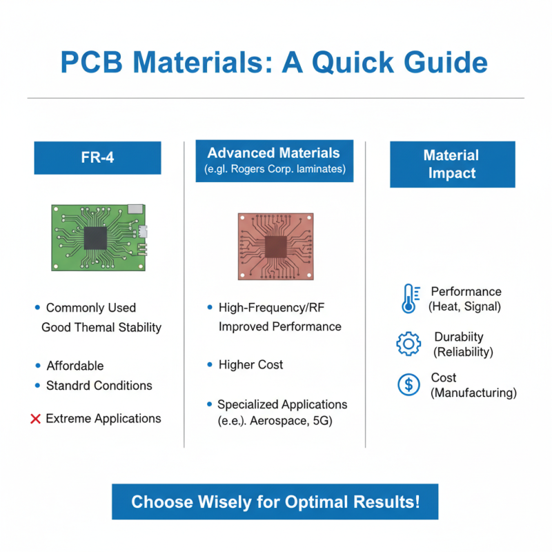
Understanding PCB materials is crucial for effective fabrication and assembly. Different materials impact performance, durability, and cost. For instance, FR-4 is commonly used for its thermal stability and affordability. However, it may not perform well under extreme conditions.
Copper is another vital component. It serves as the conductive layer on the PCB. The thickness and quality of copper affect electrical performance. Thin copper may lead to overheating issues. On the other hand, excessive thickness can increase production costs unnecessarily.
The choice of materials often comes with trade-offs. While advanced materials like Rogers may offer superior performance, they are also more expensive. This can squeeze budgets. Engineers must balance performance needs with production costs. A good understanding of material properties is essential for informed decision-making.
The Assembly Techniques Used in PCB Production
In the PCB assembly process, various techniques play crucial roles. One of the common methods is Surface Mount Technology (SMT). According to a 2020 industry report, SMT accounts for nearly 70% of all PCB assemblies. This technique allows for high-density mounting of components directly on the surface of PCBs. Additionally, it enables faster production rates, yet it can lead to challenges such as alignment issues. Precision is key, and any misalignment can result in defective circuits.
Through-hole technology is another essential technique in PCB assembly. It involves inserting component leads through holes in the PCB. While considered traditional, it remains popular for certain applications, particularly with larger components. Research indicates that around 30% of PCBs still utilize this method. However, the manual process can be labor-intensive and subject to human error. As technology evolves, balancing between automation and human oversight becomes vital.
Understanding these assembly techniques is critical for improving PCB production efficiency. Advanced techniques like robotic assembly are gaining traction, yet they bring complexity. Not all manufacturers can easily adopt these technologies due to costs and training needs. Finding the right mix of traditional and modern methods can drive better outcomes in PCB assembly.
2026 How to Understand PCB Fabrication and Assembly Process? - The Assembly Techniques Used in PCB Production
| Process Step |
Description |
Assembly Techniques |
Common Materials |
| Design |
Creating schematics and layout for the PCB. |
CAD Software |
Copper, FR-4, Kapton |
| Printing |
Applying the copper layer onto the substrate. |
Photoengraving |
Copper foil, Epoxy |
| Etching |
Removing unwanted copper to create the circuit pattern. |
Chemical Etching |
Etching solution, Copper |
| Drilling |
Creating holes in the PCB for components and vias. |
Laser Drilling |
Drill bits |
| Plating |
Depositing metal onto the surface and into the holes. |
Electroplating |
Nickel, Gold, Copper |
| Solder Mask Application |
Adding a protective layer to prevent solder from shorting connections. |
Screen Printing |
Solder mask ink |
| Component Placement |
Positioning electronic components onto the PCB. |
Pick and Place |
Resistors, Capacitors, ICs |
| Soldering |
Fusing components to the PCB using solder. |
Reflow or Wave Soldering |
Solder paste, Solder wire |
| Testing |
Verifying functionality and quality of the PCB. |
Functional Testing |
Testing equipment |
| Packaging |
Preparing PCB for shipment to customers. |
Vacuum Packaging |
Anti-static bags, Boxes |
Quality Control and Testing in PCB Manufacturing
Quality control is crucial in PCB manufacturing. Each step must ensure the circuit boards meet industry standards. Testing helps identify defects early. This prevents costly errors in later stages.
Tips: Employ automated optical inspection (AOI). It detects issues that human inspectors might miss. Regularly recalibrate testing equipment to maintain accuracy.
Assembly also requires scrutiny. Even minor faults can lead to failures. Solder joint quality is particularly vital. Poor solder can cause weak connections.
Tips: Use thermal imaging to catch overheating. Ensure proper alignment during assembly to avoid misplacement. Inspect components carefully to avoid using damaged parts.
Keeping a close eye on every detail is essential. Sometimes, mistakes are unavoidable. Learn from feedback and improve processes continuously.