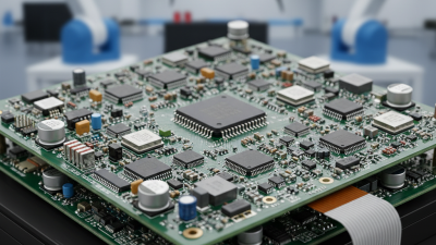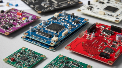
Launching a new electronic product rarely follows a straight line. A prototype may look perfect on a screen, yet fail when a connector meets a real enclosure. Prototype pcb assembly creates a controlled bridge between design files and physical evidence. Engineers can inspect solder joints, component placement, clearance, and firmware behavior before committing to larger production volumes.
Industry data supports this cautious approach. The World Semiconductor Trade Statistics (WSTS) Spring 2024 forecast projected global semiconductor sales of $611.2 billion, a 16.0% increase from 2023. More capable components also increase design interactions and manufacturing risks. IPC’s electronics manufacturing research consistently identifies material availability, labor constraints, quality, and supply-chain volatility as major industry concerns. A small, traceable assembly run can expose these problems earlier, when corrections remain affordable.
The benefits are practical. A prototype board can reveal a reversed footprint, an overheated regulator, or a connector that physically collides with the housing. Engineers can compare the assembled board against drawings, test points, and inspection records. Contract manufacturers can also provide feedback on component sourcing, stencil design, automated optical inspection, and design-for-manufacturing decisions.
It is not a shortcut.
Prototype pcb assembly does not guarantee production success. Poor documentation, rushed testing, or unsuitable components can still produce misleading results. That limitation deserves attention. However, when teams combine verified bills of materials, controlled revisions, inspection data, and realistic functional testing, prototype assembly becomes a reliable learning stage. It reduces guesswork, strengthens engineering decisions, and gives new products a more defensible path toward manufacturing.
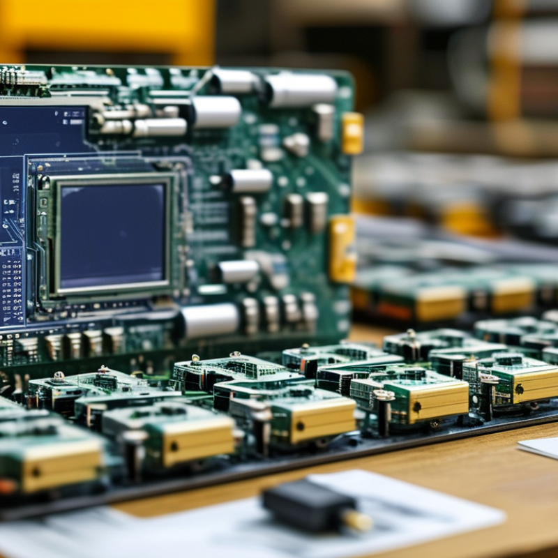
Prototype PCB assembly is the controlled production of a small batch of populated circuit boards before full-scale manufacturing. Engineers place components, solder them, and test electrical performance. The process exposes practical problems, such as poor connector access, heat buildup, or incorrect component footprints.
A prototype is more than a sample. It is physical evidence. IPC’s 2024 Electronics Industry Survey reported continued demand growth across electronics manufacturing, increasing pressure to shorten development cycles. A small assembly run helps teams verify design decisions before committing to expensive tooling and inventory. It also supports functional testing under real conditions, not only in simulation.
In practice, the first build is rarely perfect. That is normal. A missing test point or weak solder joint can appear only after assembly. Industry rework studies often show that defects discovered later cost many times more than defects found during design. The exact multiplier varies by project, so treating it as a fixed rule would be careless. Still, the lesson is clear: early feedback has measurable value.
Prototype assembly also reveals manufacturability issues. Engineers can check component spacing, inspection access, solder coverage, and programming steps. The build record should include drawings, revision codes, test results, and observed failures. Small batches cost more per board, but they create reliable learning before volume production begins.
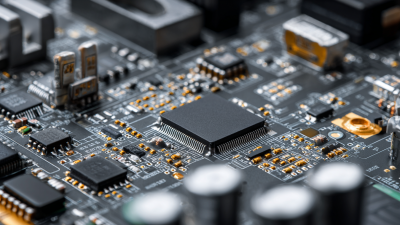
A prototype PCB assembly turns a digital design into a testable, measurable product. It helps teams verify circuit performance before committing to larger production quantities. In practical engineering work, early assembly often reveals problems hidden in schematics, such as tight clearances, incorrect footprints, or difficult soldering areas.
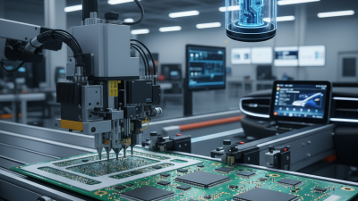
The process begins with a design review. Engineers check Gerber files, the bill of materials, component orientation, and manufacturing limits. They may adjust trace spacing, pad sizes, or connector locations before fabrication. A bare board is then produced, while a stencil prepares precise solder paste deposits. Pick-and-place equipment positions components, followed by controlled reflow heating. Through-hole parts may require selective or manual soldering.
Inspection follows assembly. Automated optical inspection can detect shifted parts, solder bridges, and missing components. X-ray inspection may be useful for hidden joints beneath certain packages. The assembled board then receives electrical checks and functional testing with cables, firmware, or simulated loads. Test results should be recorded carefully.
A useful mistake.
During one prototype review, a connector worked electrically but blocked access to a nearby screw. The circuit was correct, yet the enclosure failed. That small issue changed the layout before production. Prototype assembly is not always smooth. Component shortages, unclear drawings, or one overlooked measurement can delay testing. These setbacks are valuable when engineers document them, correct the design, and repeat the build with stronger evidence.
| Process Stage | Main Activities | Typical Time Range | Key Outputs | Quality and Engineering Checks | Why It Matters for a New Product | Typical Status |
|---|---|---|---|---|---|---|
| 1. Design and Documentation Review | Review the schematic, PCB layout, bill of materials, component specifications, assembly drawings, and manufacturing notes. | 1–3 business days | Approved manufacturing data package and list of design questions. | Design-for-manufacturing review, component availability check, polarity review, footprint verification, and missing-data identification. | Detects preventable design and documentation problems before materials and assembly work begin. | Required |
| 2. Component Sourcing | Confirm part numbers, package types, quantities, approved alternatives, and component purchasing requirements. | 2–10 business days | Verified component list, purchasing plan, and shortage report. | Lifecycle status, electrical equivalence, package compatibility, moisture sensitivity, and counterfeit-risk controls. | Prototype builds often use small quantities, making obsolete, unavailable, or long-lead-time parts easier to identify and resolve. | Supply Dependent |
| 3. PCB Fabrication | Manufacture the bare printed circuit boards according to the approved layer count, material, finish, thickness, and design files. | 3–10 business days | Bare PCBs ready for assembly. | Dimensional inspection, solder-mask and silkscreen review, pad and hole verification, surface-finish inspection, and electrical testing when specified. | Provides physical boards for validating mechanical fit, electrical behavior, and assembly compatibility. | Build Dependent |
| 4. Stencil and Assembly Preparation | Create the solder-paste stencil, prepare feeders or placement data, verify component orientation, and organize the assembly sequence. | 0.5–2 business days | Assembly setup, placement program, stencil, and work instructions. | Paste-aperture review, fiducial verification, feeder setup, orientation control, and assembly drawing confirmation. | Accurate preparation reduces placement errors and helps produce repeatable prototype results. | Required |
| 5. Solder Paste Printing | Apply solder paste to the PCB pads through a stainless-steel stencil. | Same day | PCB panels with deposited solder paste. | Paste coverage, alignment, deposit volume, bridging risk, paste storage conditions, and stencil cleanliness. | Consistent solder-paste deposits are essential for reliable surface-mount solder joints. | Controlled |
| 6. Component Placement | Place surface-mount components using automated placement equipment and install any components requiring manual handling. | Same day | Populated boards prepared for soldering. | Component value, reference designator, polarity, orientation, position accuracy, and missing-component inspection. | Prototype assembly reveals placement constraints, footprint issues, and practical assembly risks before production quantities increase. | Controlled |
| 7. Reflow and Through-Hole Soldering | Reflow solder surface-mount components and complete through-hole soldering by selective, wave, or manual methods as appropriate. | 0.5–1 business day | Soldered prototype assemblies. | Thermal-profile verification, solder-joint inspection, component heat limits, solder bridging, voiding, insufficient solder, and lifted leads. | Confirms that the selected materials, component packages, and assembly methods can withstand the soldering process. | Controlled |
| 8. Inspection and Testing | Perform visual inspection and, when required, automated optical inspection, X-ray inspection, electrical testing, or functional testing. | 1–3 business days | Inspection records, defect list, test results, and rework recommendations. | Polarity, solder quality, component presence, hidden solder joints, short circuits, open circuits, programming, and basic functional behavior. | Finds assembly defects early and provides evidence for improving the design and manufacturing process. | Required |
| 9. Rework and Engineering Changes | Correct confirmed defects, replace unsuitable components, update documentation, and record design or process changes. | 1–5 business days | Corrected boards and engineering-change log. | Root-cause analysis, reinspection after rework, traceability, and confirmation that modifications do not create new defects. | Prototype builds are intended to support learning, allowing issues to be corrected before tooling or volume production decisions. | As Needed |
| 10. Functional Validation | Power up the assembled PCB and evaluate electrical performance, interfaces, firmware behavior, thermal performance, and mechanical integration. | 1–20 business days | Validation data, test reports, failure analysis, and revision recommendations. | Operating voltage, current consumption, signal integrity, temperature behavior, communication interfaces, safety limits, and user requirements. | Shows whether the prototype meets its intended requirements and identifies changes needed for the next revision. | Product Dependent |
| 11. Design Revision | Update the schematic, PCB layout, bill of materials, firmware, assembly instructions, and test procedures based on test findings. | 2–15 business days | New revision package and updated change history. | Revision control, design-rule verification, component substitution review, and confirmation that corrective actions address the failure cause. | Shortens the path from an initial concept to a more manufacturable and reliable product design. | Iteration Based |
| 12. Prototype Review and Production Planning | Evaluate yield, defects, assembly time, test coverage, material availability, and production risks before a larger build. | 1–5 business days | Production-readiness checklist and recommended next-build actions. | First-pass yield, defect trends, test coverage, process capability indicators, supply continuity, and documentation completeness. | Creates a fact-based decision on whether to proceed, revise the design, or conduct another prototype build. | Decision Point |
Prototype PCB assembly gives new product development a practical testing ground. Engineers can verify circuit behavior, component fit, thermal performance, and assembly access before committing to volume production. In a pilot build, a misplaced connector or weak solder joint becomes visible on the bench, not in a customer’s hands. That experience is valuable, although the first prototype is rarely perfect.
Supply-chain learning is another major benefit. A U.S. Department of Commerce semiconductor supply-chain report found that chip inventories fell from about 40 days in 2019 to fewer than five days in 2021. Prototype assembly helps teams check substitute components early, before shortages disrupt production schedules. It also exposes purchasing risks, footprint errors, and unavailable parts while changes remain affordable.
Small batches cost more per board. They can prevent larger losses later.
Prototype assembly supports measurable engineering decisions. Teams can compare test results, record failure modes, and refine the bill of materials with evidence. The 2020 Global Value Chain Resilience Survey reported that 93% of supply-chain leaders planned to increase resilience. A controlled prototype build supports that goal through local inspection, traceable revisions, and documented process feedback.
Yet prototypes can create false confidence. Limited samples may not reveal long-term heating, vibration, or supplier variation. Engineers should test beyond basic function, even when the schedule feels uncomfortable.
Choose prototype PCB assembly when your design still carries unanswered questions. This stage suits new circuits, dense layouts, fine-pitch packages, and products needing early compliance checks. Engineers can inspect solder joints, connector fit, thermal behavior, and firmware performance before committing to volume tooling.
Industry data supports this cautious approach. The 2024 Global R&D Funding Forecast estimates worldwide research and development spending above 3 trillion dollars. Much of that investment depends on reducing development waste. IPC technical guidance also emphasizes controlled assembly processes, documented inspection, and workmanship requirements based on IPC-A-610. A prototype build creates evidence for those decisions.
Use it after schematic review and PCB layout verification, but before large purchasing commitments. A small batch of 5 to 50 boards can reveal reversed polarity, insufficient test points, or a connector that is awkward to reach. Automated optical inspection and X-ray inspection may expose hidden solder defects. These details matter.
Prototype assembly is not always the cheapest option. Hand assembly may appear faster for simple boards. That assumption can fail when rework consumes engineering hours. In practice, the best timing depends on component availability, board complexity, and the cost of one field failure. Leave room for mistakes. Early builds should test assumptions, not merely confirm optimism. Documentation should record every change, including substitutions, rework, and unresolved risks.
Prototype PCB assembly is valuable when a design needs physical proof, not just simulation. Before requesting a build, review the bill of materials, component availability, package sizes, and approved substitutes. The U.S. Department of Commerce reported that semiconductor inventories fell from about 40 days in 2019 to fewer than five days in 2021. A prototype using unavailable parts can delay learning.
Plan the assembly method early. Surface-mount density, through-hole parts, fine-pitch packages, and solder access affect cost and yield. Include test points, programming access, inspection requirements, and a clear revision code. IPC guidance emphasizes controlled documentation and process verification for reliable electronic assemblies. Small omissions matter. A missing polarity mark can create avoidable rework.
Use the prototype to challenge the design, not merely confirm it. McKinsey Global Institute estimated that supply-chain disruptions can erase 45% of one year’s profits over a decade. Early assembly can expose weak sourcing, thermal problems, connector strain, or poor test coverage before volume production. However, a prototype is not a miniature production run. Its results may mislead if materials, assembly equipment, or inspection methods differ later. Leave room for one imperfect iteration. That deliberate correction is often more valuable than a rushed first pass.